인텔® 아톰™ 프로세서 Z6xx 시리즈(인텔® SM35 익스프레스 칩셋 포함)
Oak Trail (Lincroft + Whitney Point)
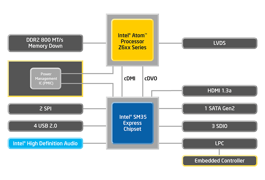
☞ 개요
인텔® 아톰™ Z670 및 Z650 프로세서는 45nm 공정 기술에 기반한 고급 전원 관리 기술을 구현하여 탁월한 와트당 성능 수준을 제공합니다. 인텔® SM35 익스프레스 칩셋과 함께 사용할 경우 이 플랫폼의 저전력, 배터리 지원 기능 및 임베디드 태블릿 디자인이 한층 최적화됩니다.
•인텔® 아톰™ 프로세서 Z6xx 시리즈는 에너지 효율이 뛰어난 단일 인텔® 아톰™ 프로세서 코어와 3D 그래픽, 비디오 디코딩 가속 기능, 메모리 및 LVDS 디스플레이 컨트롤러를 하나의 패키지로 결합합니다.
•인텔® 통합 그래픽 미디어 가속기(GMA) 600 그래픽 엔진: 400MHz 그래픽 코어 주파수에서 작동하며, 전력 최적화된 2D/3D 그래픽 엔진은 Microsoft Windows* DX9, Linux* OpenGL 2.1 및 하드웨어 가속 HD 비디오 디코딩을 지원합니다.
•통합형 메모리 컨트롤러 및 DDR2 지원: 통합형 32비트 단일 채널 메모리 컨트롤러는 효율적인 사전 반입 알고리즘, 낮은 지연 및 높은 메모리 대역폭을 통해 빠른 메모리 읽기/쓰기 성능을 제공합니다. 이 프로세서 시리즈는 최대 2GB 용량의 DDR2 800MT/s 메모리 기술을 지원합니다.
•우수한 인텔® SM35 익스플레스 칩셋을 채택하고 있으며, 이 칩셋이 내장된 14x14mm 493-볼 FCBGA 패키지에는 HDMI v1.3a 및 HDCP 1.3 호환 디스플레이 출력 기능과 WiFi, WWAN 및 LAN 솔루션 및 SSD 호환 SATA Gen 2를 지원하는 USB 및 SDIO 포트가 포함되어 있습니다.
•이 플랫폼은 Windows*7, Windows Embedded Standard* 7, MeeGo* 1.2 및 Android* 3.x(Honeycomb*)를 비롯한 다양한 운영 체제를 지원합니다.
프로세서
| 프로세서 번호 | 캐시,클록속도 | 전력 | 메모리 | 제품 기술 | | 인텔® 아톰™ 프로세서 Z650 | 512 KB, 1.2 GHz | 3.0W | 2 GB, DDR2 800 | HT | | 인텔® 아톰™ 프로세서 Z670 | 512 KB, 1.5 GHz | 3.0W | 2 GB, DDR2 800 | HT |
칩셋
| 제품 | 패키지 | 전력 | 기능 | | 인텔® SM35 익스프레스 칩셋 | 493-ball FCBGA 14x14mm | 0.75W | HDMI v1.3a 및 HDCP 1.3, USB 2.0 4개, SDIO 3개, SPI 2개, 인텔 HDA, SATA 1개, LPC |
☞ Atom Processor Z6xx Series Features
• Supports Intel® Hyper-Threading Technology
• 2-wide instruction decode and in-order execution
• 512 KB, 8 way L2 cache
• Support for IA 32-bit architecture
• FCMB3 packaging technology
• Thermal management support using TM1 and TM2
• On die Digital Thermal Sensor (DTS) for thermal management support using Intel® Thermal Monitor 1 (TM1) and Intel® Thermal Monitor 2 (TM2)
• Advanced power management features including Enhanced Intel® SpeedStep® Technology
• Supports C0/C1(e)/C2(e)/C4(e) power states
• Intel Deep Power Down Technology (C6)
■ System Memory Support
• One channel of DDR2 memory
• 32-bit data bus
• Memory DDR2 transfer rates of 800 MT/s
• Supports 1 Gb, and 2 Gb devices
• Supports total memory size of 1 GB, and 2 GB
• Provides aggressive power management to reduce power consumption when idle
• Provides proactive page closing policies to close unused pages
■ Display Controller
• Seven display planes: Display Plane A, Display Plane B, Display C/sprite, Overlay, Cursor A, Cursor B, and VGA
• Display Pipe A: Supports LVDS display interface
• Display Pipe B: Supports HDMI via chipset
• Maximum resolution (LVDS display):
⎯ 1366 x 768 @ 18 bpp and 60 fps
• Supports 18 bpp
• Supports Non-Power of 2 Tiling
• Output pixel width: 24-bit RGB
• Supports NV12 video data format
• Supports 3 x 3 panel fitter
• Dynamic Power Saving Technology (DPST) 3.0
• Support 16 x 256 byte tile size
• Supports overlay
• Supports global constant alpha blending
■ cDMI
• Peak raw BW of cDMI link per direction = 400 MT/s using a quad-pumped 8-bit transmit and an 8-bit receive data bus
• Supports low power management schemes
• Supports CMOS interface
■ cDVO
• Peak raw BW of 800MT/s
• Supports low power management schemes
• Supports AGTL+ interface
■ LVDS
• Maximum resolution (internal display) of:
• 1366 x 768 @ 18 bpp and 60 fps
• Dot clock range from 20–83 MHz
• Four differential signal pairs: Three data pairs (up to 581 Mbps on each data link) and one clock pair
• Supports 18 bpp packed and 18 bpp loosely packed pixel formats
• Supports 24 bpp with a limited number of validated panels.
☞ Platform Controller Hub(PCH) SM35 Features
• CMOS Direct Media Interface (cDMI)—Primary link between Processor and PCH
• CMOS Digital Video Out (cDVO)—Display Interface between Processor and PCH for driving external displays.
• Universal Serial Bus (USB) High Speed (HS)—In the box USB HS device interface
• One SD/SDIO/MMC interface
• One dedicated SDIO communication interface.
• Intel® HD Audio 1.0 Interface with two SDIs
• One HDMI 1.3a interface for external display
• Single ported AHCI 1.3 compliant SATA host controller with support for up to 3.0 Gbs (Gen2) transfer rate
• Three I2C interfaces to allow monitoring in-box environmental sensors and to control in-box components
• Two SPI master interfaces to interface with simple external devices (e.g., the touch screen controller or GPS device)
• Protocol/voltage level converters for external displays
• The system clock generator providing clocks for all components in the system except for the real-time clock.
• System Controller Unit (SCU)—Provides platform power management by use of PMIC and management system standby states
• Intel Legacy Block t(iLB) hat includes the following blocks
— LPC
— 8254
— 8259
— RTC
— IOAPIC
• Support for ACPI 1.3 configuration and power managementSRAM—A 256-KB block of SRAM used for system boot code and other functions when system DRAM (connected to Processor) is unavailable.
— This allows the processor to extend standby time and enhances battery life.
• DFx—Design for Test/Debug
— Boundary Scan
— JTAG access to System Controller Unit (SCU) to support power management and boot debug
☞ Platform Brief: Intel® Atom™ Processor Z6xx Series with Intel® SM35 Express Chipset
|
|